RAMP GENERATOR
Schematic:
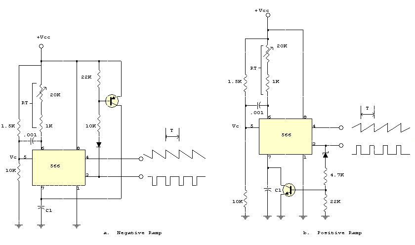
Notes:
The 566 can be wired as a
positive or negative ramp generator. In the positive ramp generator, the
external transistor driven by the Pin 3 output rapidly discharges Cl at the end of the charging period so that charging can
resume instantaneously. The pnp
transistor of the negative ramp generator likewise rapidly charges the timing
capacitor Cl at the end of the discharge period.
Because the circuits are reset so quickly, the temperature stability of the
ramp generator is excellent. The period
T is 1/2 fo
where f, is the 566 free-running
frequency in normal operation. Therefore,
T =
1 = Rt C1 Vcc
2fo 5(Vcc - Vc)
where Vc
is the bias voltage at Pin 5 and Rt is the total
resistance between Pin 6 and Vcc. Note that a short pulse
is available at Pin 3. (Placing collector resistance in series with the
external transistor collector will lengthen the pulse.)
Return to Signal Circuits